Circuit board assembly involves the process of connecting various electronic components to a printed circuit board (PCB) to create a functional electronic system. Here’s a breakdown of the key steps involved:
Design and Prototyping: Engineers design the circuit layout using specialized software.
Prototyping involves creating a sample board to test the design’s functionality.
Material Preparation: Selecting and preparing the materials, including the PCB, electronic components, and soldering materials.
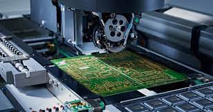
Component Placement: Mounting electronic components onto the PCB according to the design specifications.
Components may include resistors, capacitors, integrated circuits, and more.
Soldering: Soldering is the process of melting a metal alloy to create a strong electrical connection between components and the PCB.
Surface Mount Technology (SMT) or Through-Hole Technology (THT) methods may be used.
Inspection: Checking for any soldering defects, such as shorts or opens, using visual inspection or automated optical inspection (AOI) systems.
Testing: Functional testing ensures that the assembled circuit board performs as intended.
Various testing methods include in-circuit testing, functional testing, and boundary scan testing.
Cleaning: Removing any residues left from the soldering process, ensuring a clean and reliable final product.
Packaging: Once the circuit boards pass inspection and testing, they are packaged and prepared for shipment.
Quality Control: Ongoing quality control measures to ensure consistency and reliability in the manufacturing process.
Documentation: Creating documentation that includes assembly instructions, test procedures, and specifications for future reference.
The level of automation and precision in each step can vary depending on the complexity of the circuit board and the manufacturing facility’s capabilities. Advanced technologies such as robotics and automated inspection systems are increasingly being integrated into the assembly process for efficiency and accuracy.
Process involved in circuit board assembly:
Design: Engineers create a schematic and design the PCB layout using CAD software.
Material Acquisition: Source and acquire the necessary materials, including PCBs and electronic components.
Stencil Creation (for SMT): Develop a stencil for applying solder paste in Surface Mount Technology (SMT).
Component Placement: Use pick-and-place machines for SMT or manually insert Through-Hole components.
Solder Paste Application (for SMT): Apply solder paste onto the PCB through the stencil.
Soldering: Reflow soldering for SMT or wave soldering for Through-Hole components.
Visual and Automated Inspection: Inspect for defects using visual checks and automated optical inspection (AOI).
In-Circuit Testing (ICT): Test the functionality of the assembled PCB.
Functional Testing: Verify the entire system’s performance.
Cleaning: Remove flux residues or contaminants from the soldering process.
Quality Control: Implement ongoing quality checks, possibly using Statistical Process Control (SPC).
Packaging and Shipping: Package the assembled PCBs for shipment.