How to Design Your Own PCB – From Basic Layout Tips to Final Artwork
Printed circuit boards (PCBs) serve as the core platform for mounting and interconnecting electronic components in a product. Designing your own custom PCB provides immense flexibility and cost savings compared to using off-the-shelf boards.
This comprehensive guide covers the end-to-end process of DIY PCB design – from preparing the schematic, layout considerations, routing guidelines, generating fabrication and assembly files, to final artwork submission. Follow these tips to successfully design your custom PCB from concept to reality.
Step-by-Step PCB Design
1. Understand the electrical parameters.
Before starting a PCB design, you should know and understand the electrical parameters of the system, including:
Current maximums
Voltages
Signal types
Capacitance limitations
Impedance characteristics
Shielding considerations
Type and location of circuit components and connectors
Detailed net wire listing and schematic
2. Creating the schematic.
One of the first steps is always creating a schematic, which refers to the design at the electrical level of the board’s purpose and function. At this point, it’s not yet a mechanical representation.
3. Use a schematic capture tool to create your PCB layout.
The right PCB provider will work with principal engineers to develop a schematic with a software platform such as Mentor PADS®, Allegro, or Altium, which shows you exactly how your board will operate and where the components will be placed. After you create your schematic, the mechanical engineer will load the design and determine how it will fit in the intended device.
4. Design your PCB stackup.
This is important to consider early on in the PCB design stage due to impedance, which refers to how much and how quickly electricity can travel down a trace. The stackup plays a role in how the mechanical engineer can design and fit the PCB into the device.
5. Define design rules and requirements.
This step is largely dictated by standards and acceptability criteria from the IPC, which is the industry association for PCB and electronics manufacturing. These standards tell you everything you need to know regarding PCB manufacturing. An important tip: Find a PCB layout provider who is extremely familiar with IPC standards; this can help you avoid major revisions and project delays.
6. Place your components.
In many cases, the customer and PCB provider will discuss design and layout guidelines when it comes to the placement of components. For example, there may be standards indicating that certain components cannot be placed near others because they create electrical noise in the circuit. The PCB provider will have data sheets on every component (in most cases these are connectors), which will then be placed in the mechanical layout and sent to the customer for approval.
7. Insert drill holes.
This step is driven by the components and a connection. About half of the flex circuits on the market are double-sided, which means they have connection to the drill hole on the bottom layer.
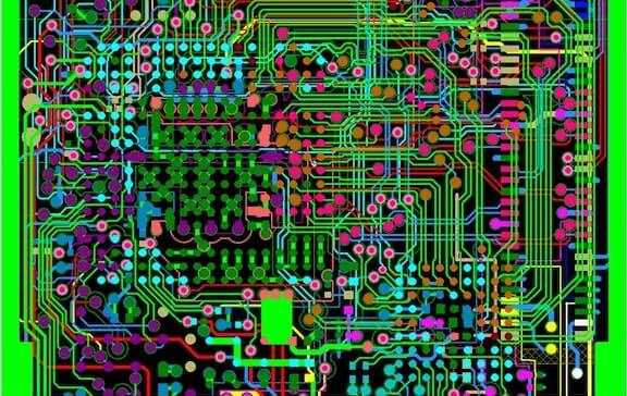
8. Route the traces.
After you’ve placed the components and drill holes, you’re ready to route the traces, which means connecting segments of the path.
9. Add labels and identifiers.
Now is the time to add any labels, identifiers, markings, or reference designators to the layout. Reference designators are helpful in showing where specific components will go on the board.
10. Generate design/layout files.
This is the final step in the layout process. These files contain all the information pertaining to your printed circuit board, and once they have been generated, your PCB is now ready for fabrication and manufacturing and assembly.
Final Checks and Finishing Touches
Run design rules check and electrical rules check on completed layout.
Review manufacturability guidelines like minimum hole size, trace spacing etc.
Examine board for any missing connections in the schematic.
Check for unrouted nets, unintended shorts, clearance violations.
Confirm via stitching, back drilling for high speed signals.
Examine decoupling capacitor placement near each IC.
Review any redundant vias, traces overlapping pads.
Rename nets, components as needed for readability.
PCB Design and Layout
Shenzhen Fumax Technology Co., Ltd is not only a professional PCB and assembly manufacturing company but also provides customers with high-quality PCB design services. Whether you are innovating in the fields of communications, healthcare, industrial, consumer electronics, or any other industry, our team is ready to help you bring your vision to life.
Our Advantages:
1.Professional Design Team
Our PCB design team consists of experienced engineers who are proficient in design and layout in circuits as well as the best practices of manufacturing and are familiar with a variety of commonly used design software.
2.One-Stop Solution Service:
We provide one-stop solution services, covering the entire process from concept to final product production. This includes shell design, hardware development, software programming, product testing and more.
3. Rapid Design Delivery
Our powerful design capability ensures the shortest possible time on PCB design. For some projects, we can complete your requirements in as little as 24 hours.
4. Manufacturing Advantage
Once the design is complete, we can directly proceed with production at our factory, helping you save a lot of time. Our manufacturing services include 3D&CNC, PCB and assembly